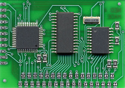
The technology is used by us is shrinking day by day drastically. We have used the devices made for the desktop PC on 180 nm or higher process. The main root level part for designing and manufacturing devices are diode, transistor, mosfet, mesfet, jfet etc. Today the main features are supplied by the mosfet. This device provides more and more features than the others. There are three main parts of this device drain, gate and source.

TO KNOW MORE ABOUT THIS PROCESS OF 28 nm SOME USEFUL LINKS
The size of the mosfet gate was 180nm or higher but today, in this era this is only 28 nm. This is so much challenging for the designers to design this devices for the upcoming latest technology at the shrinking environment. This process is going towards the pikometer range gradually.
No comments:
Post a Comment